Sunday, July 21, 2019

Filler cells and why well continuity is needed in vlsi ?


What is continuity, why it is needed?
There are 3 types of continuity: N-well, P-well  & power  continuity without continuity, the design rules dictate that you will need to space things further apart. Also, the wells need to be tied to a single global VDD/VSS so as to tap power only at one point anywhere in the standard cell row. Thus, all the wells & power lines of individual standard cells have to be tied to maintain continuity.

N-well continuity:
It is a fabrication issue. Creation of mask is costly. If you have single N-well mask, you can easily fabricate. If you separate N-well masks, there is chances of Well Proximity Effects (WPE) which may vary electrical parameters of your device.
1. What is the need for filler cells??
In standard cells APR flow, the cells in the design are placed on the row. To make sure that each cells gets power and ground connection, the cells are abutted together son that the VDD and VSS terminal of neighboring cells short together. This makes it possible to tap power only at one point anywhere in the row. But it is virtually impossible to fill 100% of the die area with regular cells. So we use filler cells to fill there spaces between regular library cells to route power rails.

  • Filler cells are used for connecting the gaps between the cells after placement.
2. What are filler cells ?
In short, Filler cells primarily are non-functional cells used to continue the VDD and VSS rails (i.e. when performing automatic PnR using standard cells there will be discontinuity in power, ground and diffusion layers because all the cells will not be abutting.).
They serve 2 main purposes:
  • They reduce the DRC violations created by the base (N-well, P-plus & N-plus) layers.
  • They help maintain the power rail connection continuity.
Filler cells are used to establish the continuity of the N-well and the implant layers on the standard cell rows. This is one of the Fab constraints, for ease in the generation of the masks.
3. When are they inserted into the PD flow?
  1. After Routing and Timing closure, but before LVS and DRC.
  2. Filling 100% of the area with regular cells is generally impossible. We need spaces to improve the placement and routing. Once we complete the routing and achieve the timing closure, we may need to fill the empty spaces with filler cells.
  3. They a re inserted into the flow after your timing, placement  opt and DRC cleanup. They are inserted to meet your utilization targets so as to avoid sagging of layers after fab and to ensure n-well continuity. Once the placement is done (after meeting the timing in PnR) you need to run command to add filler cells and tool will automatically add filler cells where ever there is empty space between standard cells.
  4. As you ask the SoC - ENCOUNTER tool to place the filler cells, it fills the gaps in the design in standard cell rows with different variety of filler cells as per the gaps availability, however there will be overlaps, you can delete the overlapping ones.
4. What will happen if we don't insert filler cells?
Basically filler cells will make power/ground and n-well continuity. There will be power/ground open between the standard cells (empty space) and also may be n-well spacing DRC error.
5. What are the other uses of Filler cells?
  1. Filler cells don't have functionality. They have power rails, N-well, P-plus, N-plus layer only. If we want to do any Engineering Change Order (ECO's) then the filler cells can be deleted and the empty spaces can be utilized. They can also be used to cope with setup or hold violations.
  2. Some filler cells have caps in them for decoupling capacitor. But De-cap cells are quite different from the filler cells, while there can as Decoupling capacitance's. Decap cells can help to reduce IR drop or reduce noise in mixed signal designs.
  3. I don't really think that filler cells can solve any metal density issues. It is usually solved by metal fill option in the tool. Metal density rule arises out of another fab constraints, to physically support the substrate minimum metal density that should be maintained throughout the die area on all the layer.
  4. Filler cells don't play any role in Latch-up prevention. For Latch-up prevention, we use TAP cells.

Tuesday, June 11, 2019

Basics of CMOS

MOSFET:
The MOS transistor, also called MOSFET (Metal-Oxide-Semiconductor Field-Effect Transistor) or IGFET (Insulated-Gate Field-Effect Transistor) is the most widely used semiconductor device and is at the heart of every digital circuit. Without the MOSFET there would be no computer industry, no digital telecommunication systems, no video games, no pocket calculators and no digital wristwatches. MOS transistors are also increasingly used in analog applications such as switched capacitor circuits, analog-to-digital converters, and filters.
The exponential progress of MOS technology is best illustrated by the evolution of the number of MOS transistors integrated in a single memory chip or single microprocessor, as a function of calendar year. Each memory cell of a dynamic random-access memory (DRAM) contains a MOS transistor and a capacitor. This exponential growth of integration density with time is known as Moore's law.
The integration density of memory circuits is about 5 to 10 times higher than that of logic circuits such as microprocessors because of the more repetitive layout of transistors in memory chips. The increase in integration density is essentially due to the reduction of transistor size.

There are two types of MOS transistors: n-channel MOSFET, p- channel MOSFET.
N-channel MOSFET: The n-channel MOSFET in which current flow is due to electron transport, and the p-channel MOSFET in which holes are responsible for current flow. A circuit containing only n-channel devices is produced by an nMOS process.
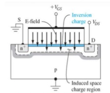
Similarly, a pMOS process fabricates circuits that contain only p-channel transistors. Today the most commonly used technology is CMOS (Complementary MOS) in which both n-channel and p-channel transistors are fabricated. Here we will limit our analysis to n-channel devices. The current-voltage expressions describing a p-channel device can readily be derived from the n-channel equations, provided the appropriate changes of sign are made. An n-channel MOS transistor is fabricated in a P-type semiconductor substrate, usually silicon. Two N-type diffusions are made in the substrate and the current flow will take place between these two diffusions. The diffusion with the lowest applied potential is called the "source" and the diffusion with the highest applied potential is called the "drain". Above the substrate, and between the source and the drain lies a thin insulating layer, usually silicon dioxide, and a metal electrode called "gate". An electron-rich layer referred to as the "channel" can be created between the source and the drain underneath the gate insulator when a positive bias is applied to the gate. With appropriate voltages applied at the source and drain electrons can then flow from the source into the drain, through the channel.

P-channel MOSFET:
In a p-channel transistor an N-type substrate is used. The P-type drain is at a lower potential than the P-type source and the application of a negative bias to the gate enables the formation of a hole-enriched channel between source and drain. The metal-insulator semiconductor structure is often referred to as a "MIS" structure, where the "I" stands for the insulator. When the insulator is an oxide, it is called a "MOS" structure.

OPERATION OF N-CHANNEL MOSFET:
The basic operation of the n-channel MOSFET is the following. We will first consider the case where the gate voltage is equal to zero while the P type substrate and the source are grounded The drain is connected to a positive voltage source for instance). Since the source and the substrate are at the same potential there is no current flow in the source-substrate junction. The drain-substrate junction is reverse biased and except for a small negligible reverse leakage current no current flows in that junction either. Under these conditions there is no channel formation, and therefore, no current flow from source to drain. In the second case a constant positive bias is applied to the gate. There is no gate current since the metal electrode is dielectrically insulated from the silicon. Because it is positively biased the gate electrode does, however, attract electrons from the semiconductor, and a thin, electron rich layer forms under the gate insulator. These electrons are supplied by the source and the drain which, being N-type, are large reservoirs of electrons. The electron-rich layer underneath the gate is called "channel". The N-type source and the N-type drain are connected by the electron rich channel, and current is now free to flow between source and drain. The effect of the gate voltage controlling the concentration of electrons in the semiconductor through the gate oxide is called "field effect". The bias on the gate creates an electric field which can either induce or inhibit the formation of an electron-rich region at the surface of the semiconductor. The terms "source", "drain", "channel" and "gate" come to mind quite naturally since the electrons originate at the source, flow through the channel and are finally collected by the drain, the whole process being controlled by the bias on the gate.
In the above equations "lamda" is Channel length modulation.


Body effect :
Body effect is major drawback of CMOS technology. This will effect when substrate or body not biased with source. There is PN-juction diode present in between substrate and source so this will effect the change of threshold voltage. in order to avoid this effect we have to give same potential to both substrate and source.
In Body effect when we give the supply voltage to the gate (+ ve) and source to (- ve) at this condition there will be formation of a diode in the reverse bias this will increase the depletion region this makes the decreasing the channel and the threshold voltage will also increases, so in order to maintain the channel we need to increase the gate voltage.
Due to this effect we are biasing the source and substrate to the same potential which will not allow the moment of depletion towards the gate by this the Threshold voltage will not be increased.


Channel Length Modulation :
To understand the Channel length modulation, first we need to know about pinch-off of the channel is introduced. The channel is formed by attraction of carriers to the gate and the current  drawn through the channel is nearly a constant independent of drain voltage in saturation mode.
As the drain voltage increases, its control over the current extends further towards source, so the uninverted region expands towards the source, shortening the length of the channel region. The effect is called Channel Length Modulation. Because resistance is proportional to length, shortening the channel decreases its resistance, causing an increase in current with increase in drain bias for a MOSFET operating in saturation region.


Monday, June 3, 2019

Short Channel Effects

The main drives for reducing the size of the transistors like their lengths, it increases speed and reducing cost. When you make circuits smaller, their capacitance's reduces, thereby increasing operating speed. In short channel there is a two - dimensional potential distribution and high electrical fields in the channel region.
  However, with great reduction of the channel there arises of short channel effects. For a given channel doping concentration, as channel length is reduced, the depletion layer widths of the source and drain junctions become comparable to the channel length. The potential distribution in the channel depends on both the traverse field ( controlled by the gate voltage ) and the longitudinal field ( controlled by the drain bias ).  When the channel of the MOSFET becomes the same order of magnitude as the depletion layer width of source and drain, the transistor start behaving differently, which impacts the performance and reliability.

The Short Channel Effects are:
1. Mobility Degradation
2. Sub-threshold current
3. Drain Induced Barrier Lowering (DIBL)
4. Surface Scattering
5. Velocity Saturation
6. Impact Ionization
7. Hot Carrier Injection

Mobility Degradation:

Mobility is important because the current in the MOSFET depends upon the mobility of charge carriers ( electrons and holes ).

The mobility can be degraded by two effects:
1. Lateral Field Effect: In short channels, as lateral field is increased, the channel mobility becomes field dependent and velocity saturation occurs. This results in current saturation.
2. Vertical Field Effect: As the vertical electric field also increases on shrinking the channel lengths, its results in scattering of carriers near the surface. Hence the surface mobility reduces.

Thus for short channels, the mobility degradation which occurs due to velocity saturation and scattering of carriers.

Sub-Threshold Current:

The sub threshold current always flows from source to drain even if the gate to source voltage is lesser than the threshold voltage of the device. This happens due to carrier diffusion between the source and drain regions of the CMOS transistor in weak inversion. When gate to source voltage is smaller than threshold voltage then leakage current will flow because of the minority charge carriers in the substrate. That makes the small current will flow from source to drain and becomes significant in the Lower Technology nodes.

Drain Induced Barrier Lowering (DIBL):

The drain potential on the channel region can have serious impact on the performance of sub-micron MOS transistors. One effect that is very similar to the punch-through effect is Drain-Induced Barrier Lowering (DIBL). In some of the books punch-through is sometimes referred to as ``subsurface DIBL'' in contrast to ``surface DIBL''.

In the weak inversion region there is a potential barrier between the source and the channel region. The height of this barrier is a result of the balance between drift and diffusion current between these two regions. If a high drain voltage is applied, the barrier height can decrease, leading to an increased drain current. Thus the drain current is controlled not only by the gate voltage, but also by the drain voltage.


For better understanding, under normal conditions when (Vds=0 and Vgs=0), there is a potential barrier that stops the electrons flow from source to drain. The gate has the function of lowering this barrier down to the point where electrons able to flow from source to drain. Ideally, the gate voltage only that would affect the barrier. As the channel becomes shorter, a larger Vd widens the drain depletion region to a point that reduces the potential barrier.

As the drain is close enough to source to easily form the depletion region normally created by the gate. That is, the drain depletion region extends to source, forming a unique depletion region this is known as punch-through.


Surface Scattering:

As the channel length becomes smaller due to the lateral extension of the depletion layer into the channel region, the longitudinal electric field component increases, and the surface mobility becomes field-dependent. Since the carrier transport in a MOSFET is confined within the narrow inversion layer, and the surface scattering (that is the collisions suffered by the electrons that are accelerated toward the interface) causes reduction of the mobility, the electrons move with great difficulty parallel to the interface, so that the average surface mobility, even for small values of, is about half as much as that of the bulk mobility.


Velocity Saturation:

The performance short-channel devices is also affected by velocity saturation, which reduces the trans-conductance in the saturation mode. At low Ey, the electron drift velocity Vde in the channel varies linearly with the electric field intensity. However, as Ey increases above 104 V/cm, the drift velocity tends to increase more slowly, and approaches a saturation value of Vde (sat) = 107 cm/s around Ey = 105 V/cm at 300 K. Note that the drain current is limited by velocity saturation instead of pinchoff. This occurs in short channel devices when the dimensions are scaled without lowering the bias voltages.


Impact Ionization:

Another undesirable short-channel effect, especially in NMOS, occurs due to the high velocity of electrons in presence of high longitudinal fields that can generate electron-hole (e-h) pairs by impact ionization, that is, by impacting on silicon atoms and ionizing them. It happens as follow: normally, most of the electrons are attracted by the drain, while the holes enter the substrate to form part of the parasitic substrate current. Moreover, the region between the source and the drain can act like the base of an NPN transistor, with the source playing the role of the emitter and the drain that of the collector. If the aforementioned holes are collected by the source, and the corresponding hole current creates a voltage drop in the substrate material of the order of 0.6 V, the normally reversed-biased substrate-source PN junction will conduct appreciably. Then electrons can be injected from the source to the substrate, similar to the injection of electrons from the emitter to the base. They can gain enough energy as they travel toward the drain to create new eh pairs. The situation can worsen if some electrons generated due to high fields escape the drain field to travel into the substrate, thereby affecting other devices on a chip.


Hot Carrier Injection:

The channel Hot Carrier effect is caused by electrons flowing in the channel for large Vds. Electron arriving at the Si-Sio2 interface with enough kinetic energy > 3.1eV to surmount the surface potential barrier are injected into the oxide. This may degrade permanently the C-V characteristics of MOSFET's.

Note: The channel hot-electron current and the subsequent damage in the gate oxide are localized near the drain junction.

The hot carrier electron induced damage in NMOS transistors has been found to result in either trapping of carriers on defect sites in the oxide or the creation of interface states at the silicon-oxide interface, or both.
The damage caused by hot carrier injection affects the transistor characteristics by causing a degradation in trans-conductance, a shift in the threshold voltage, and a general decrease in the drain current capability.

Saturday, May 11, 2019

CMOS Fabrication

Step -1: Si substrate 
Start with P- type substrate.

Step - 2: Oxidation
Exposing to high purity Oxygen and silicon at approx 1000oC in oxidation furnace.


Step - 3: Photo resist Coating
Photo resist is a light sensitive organic polymer softens when exposed to light.

Step - 4: Masking
Expose photo resist through N-well mask.


Step -5: Removal of Photo resist
Photo resist are removed by treating the wafer with acid or base solution.


Step - 6: Acid Etching
SiO2 is selectively removed from areas of wafer that are not covered by photo resist by using hydrofluoric acid.

Step - 7: Removal of Photo resist
Strip off the remaining photo resist.


Step - 8:Formation of N-well
N-well if formed with diffusion or ion implantation.


Step - 9: Removal of SiO2
Strip off the remaining oxide using HF


Step - 10: Polysilicon deposition
Deposit very thin layer of gate oxide using Chemical Vapor Deposition  (CVD) process.


Step - 11: N-Diffusion
N-Diffusion forms nMos source, drain, and n-well contact.


Oxidation


Masking

Dopants were diffusied or ion implanted.


Diffusion

Strip off oxide.


Step - 12: P - Diffusion
Similar set of steps form p+diffusion regions for pmos source, drain and substrate contact.


Step - 13: Contact cuts
The devices are to be wired together.
Cover chip with thick field oxide.
Etch oxide where contact cuts are needed.


Step - 14: Metallization:
Sputter on aluminium over whole wafer.
Pattern to remove excess metal, leaving wires.


Concepts MOS technology

Why PMOS is slower than NMOS?

The mobility of electron is more than mobility of hole. Basically free holes are present in valance band along with covalant bonds and free electrons are only present in conduction band. So free holes require more electric field to migrate as like free electrons. Because density of valance band is more than the conduction band. As PMOS having majority carriers are holes and NMOS having majority carriers are electrons these are the reasons behind speed of PMOS, NMOS.

Why CMOS is preferred over NMOS, PMOS?


In NMOS, PMOS short circuit current is flowing from VDD to GROUND for particular logic 
( nmos - logic '1', pmos - logic '0' ). So high static power is consumed on those logic's. But in CMOS short circuit current flows when both PMOS and NMOS transistors are in saturation region. This region will be very short span of time. Hence very less amount of static power will consume.

Inverter region of operation :


In this region of operations we can observe that in above diagram in one state the both PMOS and NMOS both are in the saturation region means in this state the both are in ON state. Due to this the short circuit current will flow directly from source (Vdd) to the ground (Vss) this is called as the leakage power in the CMOS.
The leakage power will be more if the input given has the high transition then the power dissipation will be more. To reduce the power dissipation the input shouldn't have high transition.

MOS Capacitor:

The MOS capacitor consists of Metal Oxide Semiconductor structure as shown. The semiconductor substrate with a thin oxide layer and a top metal contact, referred to as the gate. A second metal layer forms a  Ohmic contact to the back of the semiconductor and is called the bulk contact. The structure shown has a p-type substrate.

To understand the different bias modes of an MOS capacitor we now consider three different bias voltages. One below flat band voltage (Vfb), second between the flat band voltage and the threshold voltage (Vt) and the finally one larger than the threshold voltage. These bias are called the accumulation, depletion and inversion mode of operation.

Accumulation mode: (Vg < Vfb)
Accumulation occurs when one applies a voltage less than the flat band voltage. The negative charge on the gate attracts holes from the substrate to the oxide semiconductor interface. Only a small amount of band bending is needed to build up the accumulation charge so that almost all of the potential variation is within the oxide.

Depletion mode: (Vfb < Vg < Vt)
As a more positive voltage than the flat band voltage is applied, a negative charge builds up in the semiconductor. Initially this charge is due to the depletion of the semiconductor starting from the oxide semiconductor interface. The depletion layer width further increases with increasing gate voltage.

Inversion mode: (Vt < Vg)
As the potential across the semiconductor increases beyond twice the bulk potential, another type of negative charge emerges at the oxide semiconductor interface: this charge is due to minority carriers, which form a inversion layer. As one further increases the gate voltage, the depletion layer width barely increases further since the charge in the inversion layer increases exponentially with the surface potential.


Advantages of CMOS :
  • High input impedance : As technology shrinks, it can operate with with very low current (micro amperes). If current decreases then resistance increases ( R = V/I ).
  • Low static power consumption.
  • high packing density.
  • high noise immunity.

Friday, May 10, 2019

Latch up

What is Latch-up:

Latch up is a condition where a low impedance path is formed between the power supply and ground. By this circuit will be damaged permanently.

To understand the concept of the latch up we need to see how the NPN and PNP transistor is formed and how it operates.


As an example, in PMOS (as per Ohms's law) when the input current is low and the input nwell resistance is high then the voltage drop across resistor will high. If the voltage drop is above 0.7 v this can forward bias the Q1 transistor then it will be ON. So the output current Ic is given back to the NMOS Q2 transistor, here the input base current of the Q2 transistor is high and the input resistance is low, the drop occurred at the Q2 transistor makes ON. The output will be in the positive feed back loop this can increase the current abruptly in the circuit.  

Temperature effects (external and internal to the product) can also influence the Latch-Up immunity of products. As temperature increases, the substrate and well resistances rise allowing the bias to reach a critical value sooner. Also, the effective distance between the N+, P+ and N-Well diffusion narrows allowing easier capture of excited carriers.


                                                                  Q1- PNP transistor
                                                                  Q2- NPN transistor
                                       when Q1 (VBE >= 0.7 turns ON ), Ic= beta1 * Ib.
              The Ic current is given as input to Q2 then if it is more than VBE Q2 turns ON.
                                             The  output current (Ic) = beta2 * ( beta1 * Ib)
If beta1 * beta2 >= 1 both transistors conduct high saturation current will flow in the circuit. This damages the device. 

How to avoid Latch up condition:

1. Guard rings act as injected carrier syphons allowing these carriers to flow to the supply or ground. The Guard rings are placed around the CMOS, the spike which makes the PNP transistor turn ON that potential is absorbed by the Guard ring and it does not allow the PNP transistor to ON.
2. The resistance due to the well can be avoided by keeping parallel wire, this makes the potential spike which is occurred at the resistor will not make the Transistor to ON. 


Basics of VLSI

Introduction:

Invention of the transistor was the driving factor of growth in the VLSI technology. Before we get to know about the VLSI technology, let us have a basic knowledge of ELECTRONICS evolution. Electronics deals with circuits which involves active and passive components. These circuits are used in various Electronics Devices and are called Electronic Circuits.The components used in Electronic circuits are Diodes, Transistors, MOSFET'S. In the VLSI we will mainly concentrate on three factors they are: 1. AREA  2. POWER  3. TIMING.


Integrated Circuit:

Integrated Circuit is the circuit in which all the Passive and Active components are fabricated onto a single chip. Initially the Integrated Chip could accommodate only a few components. As the days passed, the devices became more complex and required more number of circuits which made the devices look bulky. Instead of accommodating more circuits in the system, an integration technology was developed to increase the number of components that are placed on a single chip. This technology not only helped to reduce the size of the devices but also improved the speed depending on the number of components to be integrated, they are categorized as SSI, MSI, LSI, VLSI, ULSI.

Small Scale Integration (SSI):
In this technology, 1-100 transistors were fabricated on a single chip, eg: Gates, Flip flops.

Medium Scale Integration (MSI):
Using this technology 100-1000 number of transistors could be integrated on a single chip. Eg: 4-bit micro processor.

Large Scale Integration (LSI):
Using this technology, 1000-10000 transistors could be integrated on a single chip. Eg: 8 bit Micro processor, RAM, ROM.

Very Large Scale Integration (VLSI):
In this technology, 10000-1 Million transistors could be accommodated. Eg: 16-32 bit Micro processors.

Ultra Large Scale Integration (ULSI):
In this technology, 1 Million- 10 Million transistors could be accommodated. Eg: Special Purpose Registers.

Moore's Law:

In 1965, Gordon Moore, an industry pioneer predicted that the number of transistors on a chip doubles every 18 to 24 months. He also also predicted that semiconductor technology will double its effectiveness every 18 months and many other factors grows exponentially.


Advantages of VLSI:

1. Higher Reliability
2. Increase the Operating speed of the circuit
3. Requires less power.
4. Reduces the size of the chip.