The main drives for reducing the size of the transistors like their lengths, it increases speed and reducing cost. When you make circuits smaller, their capacitance's reduces, thereby increasing operating speed. In short channel there is a two - dimensional potential distribution and high electrical fields in the channel region.
However, with great reduction of the channel there arises of short channel effects. For a given channel doping concentration, as channel length is reduced, the depletion layer widths of the source and drain junctions become comparable to the channel length. The potential distribution in the channel depends on both the traverse field ( controlled by the gate voltage ) and the longitudinal field ( controlled by the drain bias ). When the channel of the MOSFET becomes the same order of magnitude as the depletion layer width of source and drain, the transistor start behaving differently, which impacts the performance and reliability.
The Short Channel Effects are:
1. Mobility Degradation
2. Sub-threshold current
3. Drain Induced Barrier Lowering (DIBL)
4. Surface Scattering
5. Velocity Saturation
6. Impact Ionization
7. Hot Carrier Injection

The mobility can be degraded by two effects:
1. Lateral Field Effect: In short channels, as lateral field is increased, the channel mobility becomes field dependent and velocity saturation occurs. This results in current saturation.
2. Vertical Field Effect: As the vertical electric field also increases on shrinking the channel lengths, its results in scattering of carriers near the surface. Hence the surface mobility reduces.
Thus for short channels, the mobility degradation which occurs due to velocity saturation and scattering of carriers.
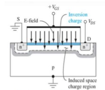
In the weak inversion region there is a potential barrier between the source and the channel region. The height of this barrier is a result of the balance between drift and diffusion current between these two regions. If a high drain voltage is applied, the barrier height can decrease, leading to an increased drain current. Thus the drain current is controlled not only by the gate voltage, but also by the drain voltage.


For better understanding, under normal conditions when (Vds=0 and Vgs=0), there is a potential barrier that stops the electrons flow from source to drain. The gate has the function of lowering this barrier down to the point where electrons able to flow from source to drain. Ideally, the gate voltage only that would affect the barrier. As the channel becomes shorter, a larger Vd widens the drain depletion region to a point that reduces the potential barrier.
As the drain is close enough to source to easily form the depletion region normally created by the gate. That is, the drain depletion region extends to source, forming a unique depletion region this is known as punch-through.


Note: The channel hot-electron current and the subsequent damage in the gate oxide are localized near the drain junction.
The hot carrier electron induced damage in NMOS transistors has been found to result in either trapping of carriers on defect sites in the oxide or the creation of interface states at the silicon-oxide interface, or both.
The damage caused by hot carrier injection affects the transistor characteristics by causing a degradation in trans-conductance, a shift in the threshold voltage, and a general decrease in the drain current capability.

However, with great reduction of the channel there arises of short channel effects. For a given channel doping concentration, as channel length is reduced, the depletion layer widths of the source and drain junctions become comparable to the channel length. The potential distribution in the channel depends on both the traverse field ( controlled by the gate voltage ) and the longitudinal field ( controlled by the drain bias ). When the channel of the MOSFET becomes the same order of magnitude as the depletion layer width of source and drain, the transistor start behaving differently, which impacts the performance and reliability.
The Short Channel Effects are:
1. Mobility Degradation
2. Sub-threshold current
3. Drain Induced Barrier Lowering (DIBL)
4. Surface Scattering
5. Velocity Saturation
6. Impact Ionization
7. Hot Carrier Injection
Mobility Degradation:
Mobility is important because the current in the MOSFET depends upon the mobility of charge carriers ( electrons and holes ).
The mobility can be degraded by two effects:
1. Lateral Field Effect: In short channels, as lateral field is increased, the channel mobility becomes field dependent and velocity saturation occurs. This results in current saturation.
2. Vertical Field Effect: As the vertical electric field also increases on shrinking the channel lengths, its results in scattering of carriers near the surface. Hence the surface mobility reduces.
Thus for short channels, the mobility degradation which occurs due to velocity saturation and scattering of carriers.
Sub-Threshold Current:
The sub threshold current always flows from source to drain even if the gate to source voltage is lesser than the threshold voltage of the device. This happens due to carrier diffusion between the source and drain regions of the CMOS transistor in weak inversion. When gate to source voltage is smaller than threshold voltage then leakage current will flow because of the minority charge carriers in the substrate. That makes the small current will flow from source to drain and becomes significant in the Lower Technology nodes.Drain Induced Barrier Lowering (DIBL):
The drain potential on the channel region can have serious impact on the performance of sub-micron MOS transistors. One effect that is very similar to the punch-through effect is Drain-Induced Barrier Lowering (DIBL). In some of the books punch-through is sometimes referred to as ``subsurface DIBL'' in contrast to ``surface DIBL''.In the weak inversion region there is a potential barrier between the source and the channel region. The height of this barrier is a result of the balance between drift and diffusion current between these two regions. If a high drain voltage is applied, the barrier height can decrease, leading to an increased drain current. Thus the drain current is controlled not only by the gate voltage, but also by the drain voltage.


For better understanding, under normal conditions when (Vds=0 and Vgs=0), there is a potential barrier that stops the electrons flow from source to drain. The gate has the function of lowering this barrier down to the point where electrons able to flow from source to drain. Ideally, the gate voltage only that would affect the barrier. As the channel becomes shorter, a larger Vd widens the drain depletion region to a point that reduces the potential barrier.
As the drain is close enough to source to easily form the depletion region normally created by the gate. That is, the drain depletion region extends to source, forming a unique depletion region this is known as punch-through.
Surface Scattering:
As the channel length becomes smaller due to the lateral extension of the depletion layer into the channel region, the longitudinal electric field component increases, and the surface mobility becomes field-dependent. Since the carrier transport in a MOSFET is confined within the narrow inversion layer, and the surface scattering (that is the collisions suffered by the electrons that are accelerated toward the interface) causes reduction of the mobility, the electrons move with great difficulty parallel to the interface, so that the average surface mobility, even for small values of, is about half as much as that of the bulk mobility.

Velocity Saturation:
The performance short-channel devices is also affected by velocity saturation, which reduces the trans-conductance in the saturation mode. At low Ey, the electron drift velocity Vde in the channel varies linearly with the electric field intensity. However, as Ey increases above 104 V/cm, the drift velocity tends to increase more slowly, and approaches a saturation value of Vde (sat) = 107 cm/s around Ey = 105 V/cm at 300 K. Note that the drain current is limited by velocity saturation instead of pinchoff. This occurs in short channel devices when the dimensions are scaled without lowering the bias voltages.Impact Ionization:
Another undesirable short-channel effect, especially in NMOS, occurs due to the high velocity of electrons in presence of high longitudinal fields that can generate electron-hole (e-h) pairs by impact ionization, that is, by impacting on silicon atoms and ionizing them. It happens as follow: normally, most of the electrons are attracted by the drain, while the holes enter the substrate to form part of the parasitic substrate current. Moreover, the region between the source and the drain can act like the base of an NPN transistor, with the source playing the role of the emitter and the drain that of the collector. If the aforementioned holes are collected by the source, and the corresponding hole current creates a voltage drop in the substrate material of the order of 0.6 V, the normally reversed-biased substrate-source PN junction will conduct appreciably. Then electrons can be injected from the source to the substrate, similar to the injection of electrons from the emitter to the base. They can gain enough energy as they travel toward the drain to create new eh pairs. The situation can worsen if some electrons generated due to high fields escape the drain field to travel into the substrate, thereby affecting other devices on a chip.Hot Carrier Injection:
The channel Hot Carrier effect is caused by electrons flowing in the channel for large Vds. Electron arriving at the Si-Sio2 interface with enough kinetic energy > 3.1eV to surmount the surface potential barrier are injected into the oxide. This may degrade permanently the C-V characteristics of MOSFET's.Note: The channel hot-electron current and the subsequent damage in the gate oxide are localized near the drain junction.
The hot carrier electron induced damage in NMOS transistors has been found to result in either trapping of carriers on defect sites in the oxide or the creation of interface states at the silicon-oxide interface, or both.
The damage caused by hot carrier injection affects the transistor characteristics by causing a degradation in trans-conductance, a shift in the threshold voltage, and a general decrease in the drain current capability.

No comments:
Post a Comment